
Advanced Certification Course in Sensor Technologies and Chip Design - IISC

- Duration
5 months, 150 hours of learning
- Mode
Live Online Classes and Campus Visits
- Commencement Date
June 21, 2025
- Application Closure Date
Closed
- Session Timings
Session 1- Saturday, 6:00 pm - 7:30 pm & 7:45 pm - 9:15 pm
- Session Timings
Session 2- Sunday, 9:00 am to 12: 15 Noon
Programme Overview
Sensor technologies and digital chip design are driving innovation across industries, enabling smarter, more efficient systems. From MEMS fabrication to AI-integrated sensors, advancements in this domain open doors to automation and intelligent decision-making. This exclusive advanced certification programme equips professionals with cutting-edge expertise in sensor technologies and chip design. The curriculum combines foundational principles with advanced applications, including MEMS fabrication, VLSI design, and AI-driven solutions. Participants gain hands-on experience with tools like COMSOL for FEM simulations and delve into additive manufacturing for custom electronic casing. The programme emphasizes the integration of AI, image processing, and sensors, enabling participants to create solutions for automated decision-making. Through a blend of theory, lab sessions, and case studies, this programme prepares participants to lead innovations across domains like healthcare, automotive systems, and consumer electronics, positioning them as leaders in the future of engineering.
Admission Criteria

Eligibility Criteria
- Education Qualification: Should have completed B.Tech./B.E/M.Sc./M.E./M.Tech. in Electronics, Electrical, Mechanical, Instrumentation, Physics, Materials Engineering/Science, Chemical Engineering or similar.
- Work Experience: 6 months (preferred, but not mandatory).
Selection Process
- Candidates will be shortlisted based on the Programme Directors’ discretion.
Who can attend?
- Working professionals and recent graduates keen to build a career in Sensor Technologies, Digital Design, FPGA Programming, Chip Design, Electronic Product Design, and Artificial Intelligence for sensors.
About IISc
IISc (Indian Institute of Science) is India’s oldest and finest higher education institute, renowned for its contributions to science, technology, and engineering. Established in 1909, it is dedicated to advancing knowledge through cutting-edge research and high-quality education across multiple disciplines. IISc is one of the first three publicly funded institutions to be granted the prestigious Institute of Eminence status by the Government of India. It has consistently ranked among the top institutions globally for its research output, innovation, and academic excellence.
The institute’s rigorous academic programs, world-class faculty, and state-of-the-art research facilities attract students and researchers from across the globe. IISc’s alumni network is vast and influential, with graduates holding prominent positions in academia, research, and industry worldwide. By fostering interdisciplinary collaborations and addressing critical global challenges, IISc continues to play a pivotal role in shaping the future of science and technology.
About CCE
The Centre for Continuing Education (CCE) was established in 1975-76 with the primary objective of providing continuing education to individuals in universities, research and development (R&D) laboratories, and industries, leveraging the resources of the Institute. The courses offered are meticulously designed to cater to the needs of diverse target groups, ranging from high school teachers to research scientists and engineers, empowering graduate engineers and scientists to evolve into competent and creative managers in technology-driven and data-centric organizations. Over the years, the CCE has significantly expanded both the scope and depth of its offerings. The CCE is committed to evolving effective teaching norms and methods, providing educational services, conducting workshops, designing specialized courses, organizing tests and examinations, and issuing appropriate grading certificates to participants, all in accordance with the Institute’s established standards.
Programme Highlights
Get Certified by Centre for Continuing Education (CCE) at IISc
Master Sensor Technology: Design, MEMS, FEM simulations expertise
Collaborative Learning: Build networks through peer interaction
Industry-Relevant Curriculum: Case studies aligned with market needs
World-Class Facilities: Practical learning in advanced cleanrooms
Flexible Learning: Live online classes for professionals
Advanced Technical Mastery: Specialize in Chip Design, CMOS, Logic Families, and microengineered device integration
Hands-On Experience: World-class experience in cleanroom environments (1,000/10,000), laboratory access, and micro-fabrication
Admission Process
- 1
Eligibility of Applicant
- 2
Application Submission
- 3
Screening & Shortlisting
- 4
Admission & Fee Payment
- 5
Book your Seat
Unleash the benefits that await you with Jaro Value adds.
%
higher employee retention rate
%
increase in employee productivity
%
higher incomes per employee
%
businesses achieved measurable growth
Companies that already trust us!
Syllabus Breakdown
- Overview of Sensors and Transducers
- Sensors and Transducer Characteristics: accuracy, precision, sensitivity, specificity, resolution, and selection criteria
- Overview of MEMS, Integration of mechanical elements, sensors, actuators, and electronics
- Importance and role of sensors and transducers in engineering fields (e.g., Industry and Biomedical applications)
- Overview of various sensor types: Temperature sensor, Motion sensor, Hall effect sensor, pMUTs and cMUTs, UV sensor, IR sensor, Pressure sensor
- Sensor Interfacing: Customized PCB Design
- Thermal Oxidation
- Diffusion and Ion Implantation
- Deposition Techniques: Physical Vapour Deposition Techniques (PVD) (E-Beam evaporation, Thermal evaporation, and Sputtering), Chemical Vapour Deposition (CVD).
- Lithography and Patterning Techniques for Sensor Fabrication
- Introduction to Bulk Micromachining & Surface Micromachining
- Etching Techniques: Wet etching and Dry etching
- Characterization Techniques – STM, AFM, Spectroscopy, XRD
-
Overview of electronic system design consideration for sensors
-
Amplifiers Types (Differential, Instrumentation, and Nonlinear Amplifiers) and Topologies used in Sensing systems and their Practical Applications
-
Unilateral negative Feedback, Linear and Frequency-independent Amplifiers used in Sensing systems
-
Active Filters and Noise removal in Sensor Amplifiers
-
Static and dynamic error in Sensor Amplifiers and their Compensation in Sensor Amplifiers
- Introduction to the world of finite element method (FEM) using COMSOL Multiphysics
- Learn how to build geometry and meshing, apply physics, set up studies and analyze results
- Learn how to do step-by-step Multiphysics analysis from a simple problem to a fully coupled Multiphysics model
- Hands-on demo on various sensors and actuators – Piezoresistive, Piezoelectric, Electromechanical, Pressure-based, Inertia-based, Thermal actuators
- Parameter optimization and performance analysis through simulations
- System integration of sensors – key concepts and challenges
- “Statistical analysis for sensor characterization – deep dive” and hypothesis testing with an example
- Model based System Engineering (MBSE) – how to do structured system design around a packaged sensor?
- Hands on with SysML and papyrus
- Introduction to Piezoelectricity and ultrasound waves
- Ultrasound imaging modes
- Medical and Industry Applications
- Image formation and quality metrics
- Beamforming and image reconstruction
- Field measurements and cavitation
- Introduction to VLSI and ASIC Design: Moore’s law, scaling technique
- Introduction to CMOS technology
- Design rules and layout techniques for CMOS implementation
- Introduction to Verilog/VHDL for hardware description
- Low-power design techniques: voltage scaling, clock gating, and power gating
- Energy-efficient circuit design strategies for battery-powered applications
- Advanced Memory Design like SRAM, DRAM, FLASH, etc.
- Timing Analysis and Signal Integrity
- Design for Testability (DFT) and Verification
- Basics IC Design flow: From RTL to GDS Overview
- Programmable devices – Field Programmable Gate Array (FPGA)
- Verilog constructs: Programming concepts (for, if-else, etc.), Vectored signals, Generic statements
- Verilog Examples based on Digital Logic, including Decoders, Encoders, Moore, and Mealy Finite state machines, Counters, FIFO, etc.
- Construction of MOSFET
- Operation of MOSFET: I-V characteristics, Non-ideal IV Effects
- CMOS Inverter: Static CMOS DC Characteristics, Beta Ratio effects, Noise margin, Delay, and Power computation
- CMOS Circuits: Static CMOS circuits and other logic families such as Domino logic, Pseudo NMOS, Pass Gate logic
- Comparison of Static CMOS and other circuits
- Design and analysis of logic gates and other And-OR-Invert and Or-And-Invert logic Circuits; Design of 4×16 Decoder as an Example.
- Delay analysis: Elmore delay models and Logical Effort — Finding the best number of stages, finding the best design with leads to minimum delay.
- Static Timing Analysis of Digital Circuits including Setup, Hold time violations
- Memory design: 6T and 8T SRAM memory cell, design, analysis, noise margins, and peripherals.
- Introduction to cleanroom protocols and equipment
- Hands-on training on various cleanroom equipment: Thermal and E-beam Evaporation tool, Sputtering tool, Mask aligner, Wire bonder, and Wet benches
- Hands-on training on soft lithography technique and 3D printing
- Sessions on sensor interfacing and analog circuit design
Programme Fee Details

- Campus visit fee will be based on actuals and to be borne by the participants.

- Fees paid are non-refundable and non-transferable.
- The total fee mentioned above includes lab charges as well.
- *18% GST extra as applicable.
Application Fee
INR 2000 + 18% GSTTotal Programme Fee
INR 2,70,000/- + GSTInstallment Pattern

- Campus visit fee will be based on actuals and to be borne by the participants.

- Fees paid are non-refundable and non-transferable.
- The total fee mentioned above includes lab charges as well.
- *18% GST extra as applicable.
Instalment 1
INR 1,35,000/- + GST As mentioned in the offer letterInstalment 2
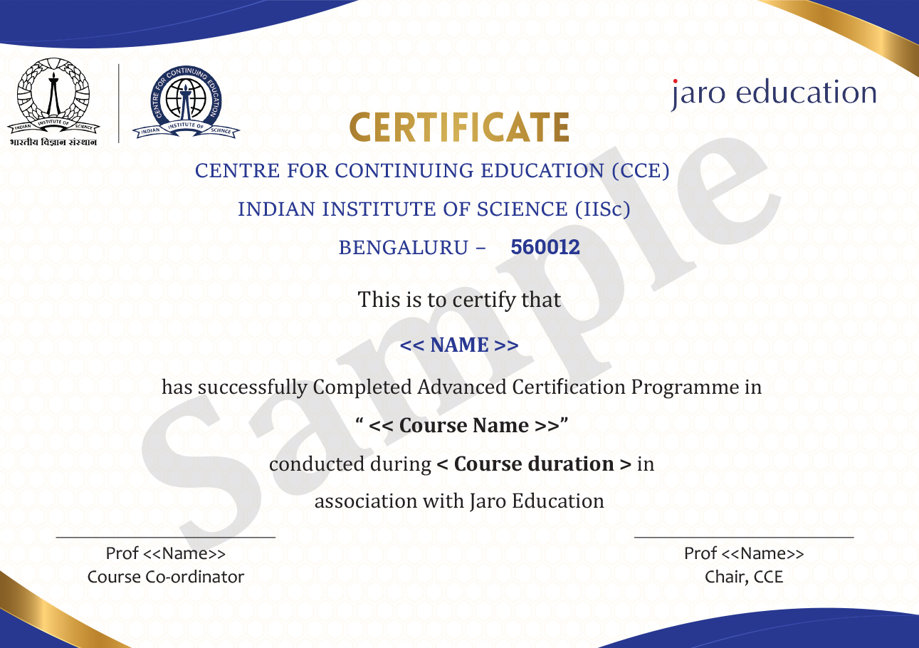
INR 1,35,000/- + GST 3rd month from programme commencementEarn a Career Certificate
- To receive a Completion Certificate, attendees must have more than 70% attendance and score above 50%. A Participation Certificate is awarded to those with more than 50% attendance and a score above 35%. No certificate is given if attendance is below 50% or marks are below 35%.
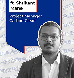
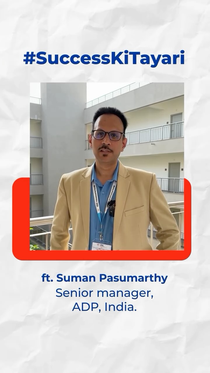
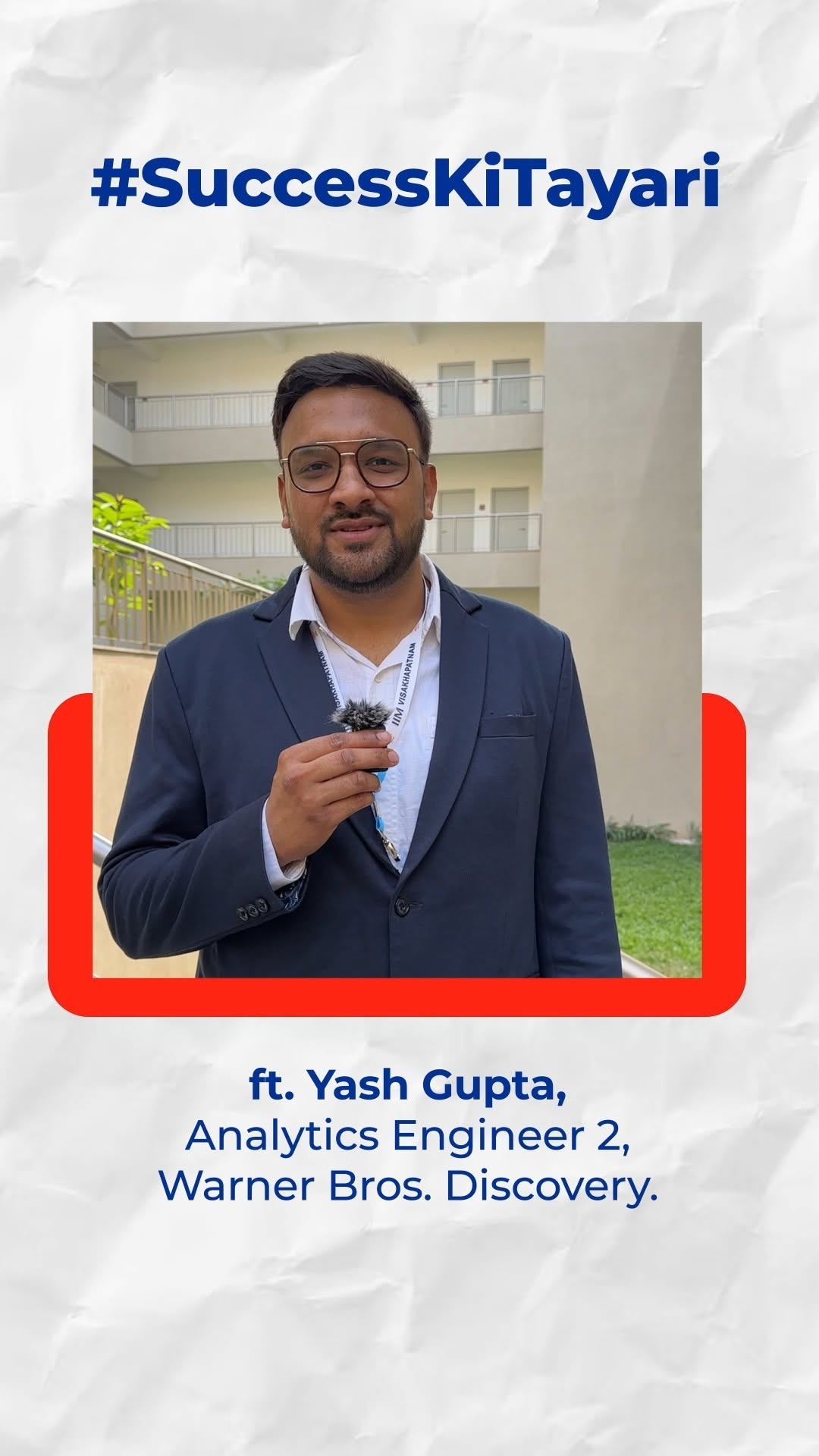
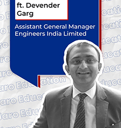
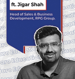
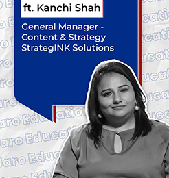
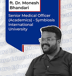
Know the Facilitators


#YouInspireUs
The Jaro Advantage

Personalized Learning Support
- Career Acceleration: Get unmatched career guidance, resume-building workshops, and 1:1 mentorship to fast-track your professional growth.
- 24/7 Student Support: Dedicated assistance at every step—from enrollment to graduation.
- Future-Ready Learning: Engage in immersive, industry-aligned programs designed for lifelong career relevance.

Expert-Led Doubt Resolution
- Learn from the Best: Access mentorship from top-tier faculty and industry leaders.
- Collaborative Learning: Join dynamic discussion forums and peer-to-peer networks for deeper insights.
- Real-World Problem Solving: Apply knowledge through case studies and interactive sessions.
Powerful Global Networking
- Elite Alumni Community: Connect with 350,000+ professionals worldwide for career opportunities and collaborations.
- Exclusive Events: Attend global webinars, networking meetups, and industry talks.
- Lifelong Access: Stay updated with cutting-edge trends and alumni benefits long after graduation.
Unlock Your Path to Success
Unsure about which course to choose? We understand—selecting the right programme can feel overwhelming. That’s why our intuitive Course Finder is here to help you discover the perfect match based on your skills, goals, and interests. Let us guide you toward your next career milestone with confidence.
Find My Ideal Course Find My Ideal Course

Refer & Earn – Amazing Rewards Await!
Share the gift of education—refer your friends and colleagues now! Earn fantastic rewards for every successful referral and empower others to advance their careers while you benefit.
Start Referring Today! Start Referring Today!