PG Level Advanced Certification Programme in
Sensor Technologies and Chip Design
- IISc

Duration
5 months, 150 hours of learning
Mode
Live Online Classes
and Campus Visits
Commencement Date
June 8, 2025
Application Closure Date
May 31, 2025
Session Timings
Session 1- Saturday, 6:00 pm - 7:30 pm &
7:45 pm - 9:15 pm
Session 2- Sunday, 9:00 am to 12: 15 Noon

Programme Overview

Sensor technologies and digital chip design are driving innovation across industries, enabling smarter, more efficient systems. From MEMS fabrication to AI-integrated sensors, advancements in this domain open doors to automation and intelligent decision-making. This exclusive PG-level certification programme equips professionals with cutting-edge expertise in sensor technologies and chip design. The curriculum combines foundational principles with advanced applications, including MEMS fabrication, VLSI design, and AI-driven solutions. Participants gain hands-on experience with tools like COMSOL for FEM simulations and delve into additive manufacturing for custom electronic casing. The programme emphasizes the integration of AI, image processing, and sensors, enabling participants to create solutions for automated decision-making. Through a blend of theory, lab sessions, and case studies, this programme prepares participants to lead innovations across domains like healthcare, automotive systems, and consumer electronics, positioning them as leaders in the future of engineering.

Programme Highlights

certificate

IISc-Certified Expertise: 
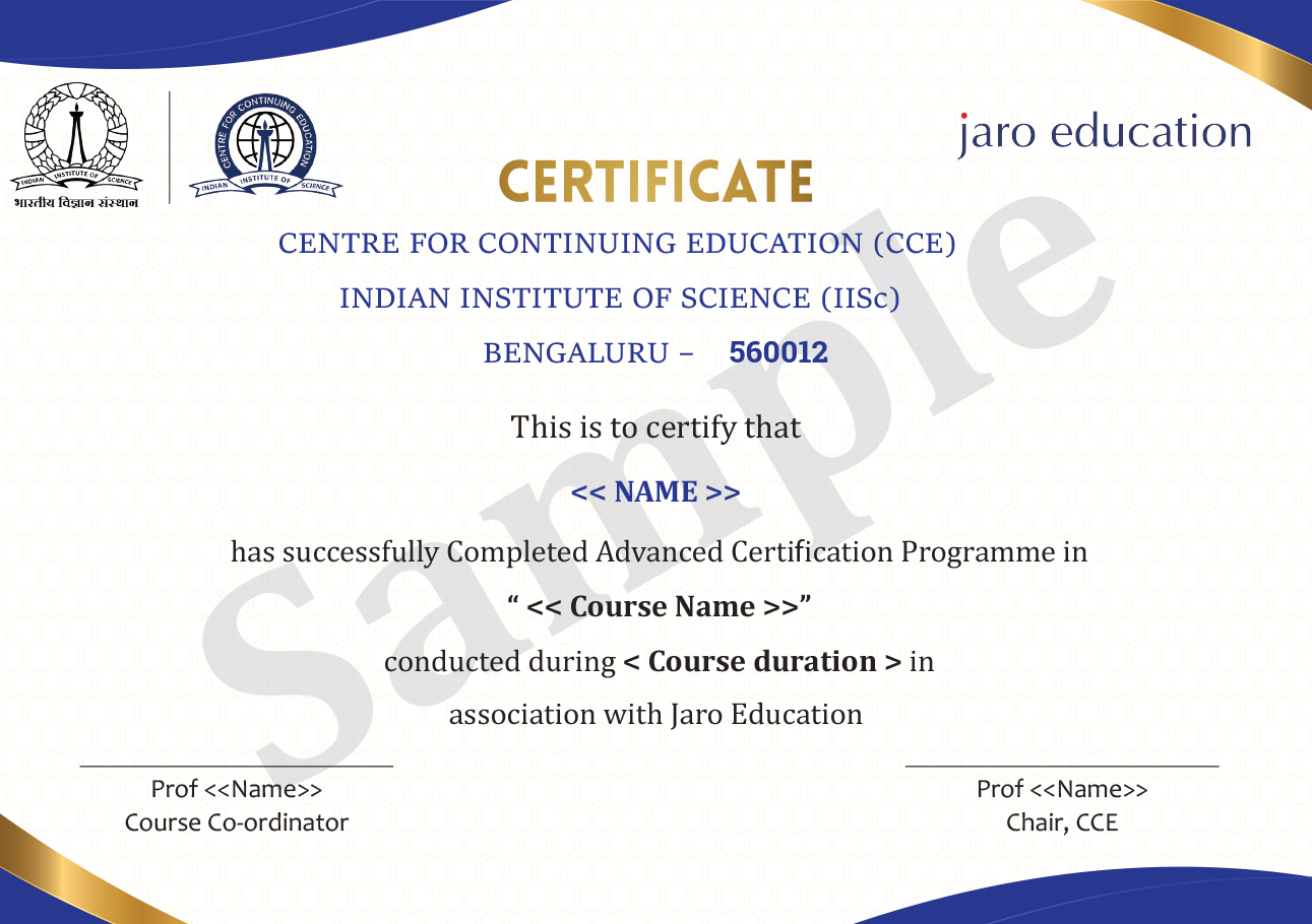
Get Certified by Centre for Continuing Education (CCE) at IISc

faculty-learning

Master Sensor Technology: Design, MEMS, FEM simulations expertise

Global Networking Opportunities

Collaborative Learning: Build networks through peer interaction

Industry-Oriented Programme

Industry-Relevant Curriculum: Case studies aligned with market needs

Theoretical and Practical Approaches

World-Class Facilities: Practical learning in advanced cleanrooms

online

Flexible Learning: Live online classes for professionals

Digital Markstrat Simulation

Advanced Technical Mastery: Specialize in Chip Design, CMOS, Logic Families, and microengineered device integration

Live classes by highly experienced faculty from IIM Nagpur

Hands-On Experience: World-class experience in cleanroom environments (1,000/10,000), laboratory access, and micro-fabrication

Eligibility Criteria

  • Education Qualification: Should have completed B.Tech./B.E/M.Sc./M.E./M.Tech. in Electronics, Electrical, Mechanical, Instrumentation, Physics, Materials Engineering/Science, Chemical Engineering or similar.
  • Work Experience: 6 months (preferred, but not mandatory).

Selection Process

  • Candidates will be shortlisted based on the Programme Directors’ discretion.

Who can attend?

  • Working professionals and recent graduates keen to build a career in Sensor Technologies, Digital Design, FPGA Programming, Chip Design, Electronic Product Design, and Artificial Intelligence for sensors.

Syllabus Breakdown

Explore the evolving space of sensor technologies and chip design from application, design and fabrication to its real-world applications:

  • Overview of Sensors and Transducers​
  • Sensors and Transducer Characteristics: accuracy, precision, sensitivity, specificity, resolution, and selection criteria​
  • Overview of MEMS​, Integration of mechanical elements, sensors, actuators, and electronics​​
  • Importance and role of sensors and transducers in engineering fields (e.g., Industry and Biomedical applications)​
  • Overview of various sensor types: Temperature sensor, Motion sensor, Hall effect sensor, pMUTs and cMUTs, UV sensor, IR sensor, Pressure sensor​
  • Sensor Interfacing: Customized PCB Design ​

​

  • Thermal Oxidation​
  • Diffusion and Ion Implantation​
  • Deposition Techniques: Physical Vapour Deposition Techniques (PVD) (E-Beam evaporation, Thermal evaporation, and Sputtering), Chemical Vapour Deposition (CVD).​
  • Lithography and Patterning Techniques for Sensor Fabrication​
  • Introduction to Bulk Micromachining & Surface Micromachining​
  • Etching Techniques: Wet etching and Dry etching​
  • Characterization Techniques – STM, AFM, Spectroscopy, XRD​
  • Overview of electronic system design consideration for sensors​

  • Amplifiers Types (Differential, Instrumentation, and Nonlinear Amplifiers) and Topologies used in Sensing systems and their Practical Applications​

  • Unilateral negative Feedback, Linear and Frequency-independent Amplifiers used in Sensing systems​

  • Active Filters and Noise removal in Sensor Amplifiers​

  • Static and dynamic error in Sensor Amplifiers and their Compensation in Sensor Amplifiers​

  • Introduction to the world of finite element method (FEM) using COMSOL Multiphysics​
  • Learn how to build geometry and meshing, apply physics, set up studies and analyze results​
  • Learn how to do step-by-step Multiphysics analysis from a simple problem to a fully coupled Multiphysics model​
  • Hands-on demo on various sensors and actuators – Piezoresistive, Piezoelectric, Electromechanical, Pressure-based, Inertia-based, Thermal actuators​
  • Parameter optimization and performance analysis through simulations​
  • System integration of sensors – key concepts and challenges​
  • "Statistical analysis for sensor characterization – deep dive" and hypothesis testing with an example​
  • Model based System Engineering (MBSE) – how to do structured system design around a packaged sensor?​
  • Hands on with SysML and papyrus​
  • Introduction to Piezoelectricity and ultrasound waves​
  • Ultrasound imaging modes​
  • Medical and Industry Applications ​
  • Image formation and quality metrics​
  • Beamforming and image reconstruction​
  • Field measurements and cavitation​
  • Introduction to VLSI and ASIC Design: Moore’s law, scaling technique​
  • Introduction to CMOS technology​
  • Design rules and layout techniques for CMOS implementation​
  • Introduction to Verilog/VHDL for hardware description​
  • Low-power design techniques: voltage scaling, clock gating, and power gating​
  • Energy-efficient circuit design strategies for battery-powered applications​
  • Advanced Memory Design like SRAM, DRAM, FLASH, etc.​
  • Timing Analysis and Signal Integrity​
  • Design for Testability (DFT) and Verification​
  • Basics IC Design flow: From RTL to GDS Overview​
  • Programmable devices - Field Programmable Gate Array (FPGA)​
  • Verilog constructs: Programming concepts (for, if-else, etc.), Vectored signals, Generic statements​
  • Verilog Examples based on Digital Logic, including Decoders, Encoders, Moore, and Mealy Finite state machines, Counters, FIFO, etc.​
  • Construction of MOSFET​
  • Operation of MOSFET: I-V characteristics, Non-ideal IV Effects​
  • CMOS Inverter: Static CMOS DC Characteristics, Beta Ratio effects, Noise margin, Delay, and Power computation​
  • CMOS Circuits: Static CMOS circuits and other logic families such as Domino logic, Pseudo NMOS, Pass Gate logic​
  • Comparison of Static CMOS and other circuits​
  • Design and analysis of logic gates and other And-OR-Invert and Or-And-Invert logic Circuits; Design of 4x16 Decoder as an Example.​
  • Delay analysis: Elmore delay models and Logical Effort — Finding the best number of stages, finding the best design with leads to minimum delay.​
  • Static Timing Analysis of Digital Circuits including Setup, Hold time violations​
  • Memory design: 6T and 8T SRAM memory cell, design, analysis, noise margins, and peripherals.​

​

  • Introduction to cleanroom protocols and equipment​
  • Hands-on training on various cleanroom equipment: Thermal and E-beam Evaporation tool, Sputtering tool, Mask aligner, Wire bonder, and Wet benches​
  • Hands-on training on soft lithography technique and 3D printing​
  • Sessions on sensor interfacing and analog circuit design  ​
*Courses are subject to change at IISc’s discretion.
Live and Interactive Lectures

Mentor-assisted Hands-on sessions

Capstone Project

Capstone Projects 

Live Class Discussions

 Live Lectures by faculty  

Chamber Consulting Sessions

Industry Sessions

campus immersion

Campus Visits

IISC Logo
Nirf

India's #1 University (2016-24) & Research Institute (2021-24)

THE WUR

India's #1 University (2024)

Bharat Ratna

2 Bharat Ratna Awardees

About IISc

IISc (Indian Institute of Science) is India’s oldest and the finest higher education institute. It pursues excellence in research and education in several fields of Science and Engineering. It is one of the first three publicly funded institutes to be awarded the Institute of Eminence status. The alums of IISc hold significant academic and industry positions around the globe. IISc’s Center for Continuing Education (CCE) offers the PG Level Advanced Certification Course in Sensor Technologies and Chip Design, which is a comprehensive exploration of sensor technology. The programme empowers professionals to comprehend, design, and construct state-of-the-art sensor solutions, enabling learners to design, fabricate, analyze, and seamlessly integrate sensors, across various industries. For more information, visit – cce.iisc.ac.in.
New CCE Logo.
Nirf

India's #1 University (2016-24) & Research Institute (2021-24)

THE WUR

India's #1 University (2024)

Bharat Ratna

2 Bharat Ratna Awardees

About CCE

The Centre for Continuing Education (CCE) was established in 1975-76 with the primary objective of providing continuing education to individuals in universities, research and development (R&D) laboratories, and industries, leveraging the resources of the Institute. The courses offered are meticulously designed to cater to the needs of diverse target groups, ranging from high school teachers to research scientists and engineers, empowering graduate engineers and scientists to evolve into competent and creative managers in technology-driven and data-centric organizations. Over the years, the CCE has significantly expanded both the scope and depth of its offerings.

The CCE is committed to evolving effective teaching norms and methods, providing educational services, conducting workshops, designing specialized courses, organizing tests and examinations, and issuing appropriate grading certificates to participants, all in accordance with the Institute’s established standards.

Know The Facilitators

Programme Certification

  • To receive a Completion Certificate, attendees must have more than 70% attendance and score above 50%. A Participation Certificate is awarded to those with more than 50% attendance and a score above 35%. No certificate is given if attendance is below 50% or marks are below 35%.

NOTE: *The sample certificate is indicative. The Institute reserves the right to revise it.

Certificate IISc STCD

Programme Structure

Programme Fee
Fee Structure
Application Fee
INR 2,000/-
Total Programme Fee
INR 2,70,00/- + GST
Installment Pattern
Installment Pattern
Installment 1
INR 1,35,000/- + GST

As mentioned in the offer letter

Installment 2
INR 1,35,000/- + GST

3rd month from programme commencement

Note:-

  • Campus visit fee will be based on actuals and to be borne by the participants.
  • Fees paid are non-refundable and non-transferable.
  •  The total fee mentioned above includes lab charges as well.   
  • *18% GST extra as applicable.

Admission Process

Talk to our Expert

Fill the form to get more information.


(Privacy and Security Guaranteed)

The Jaro Advantage

Learning Support
Jaro Logog Royal Blue
Doubt Resolution
Jaro Logog Royal Blue
Networking
Jaro Logog Royal Blue

Build 21st-Century Skill set to Gain Career Edge in the VUCA World

Learn from the best minds and eminent IISc faculty members to become the next industry expert.
By clicking Start Application, you agree to our terms and conditions and our privacy policy.

You’ll learn

Frequently Asked Questions
What is the objective of this certification programme?

The programme aims to equip professionals with advanced skills in sensor technologies, MEMS fabrication, digital chip design, and AI-driven solutions, preparing them to lead innovations in industries like healthcare, automotive, and consumer electronics.

Who is this programme designed for?

This certification is tailored for engineers, researchers, and industry professionals keen on advancing their expertise in sensor technologies, VLSI design, and AI integration, especially those working in or aspiring to join semiconductor and IoT-driven industries.

What key skills will I learn in this sensor technologies and chip design programme?

Participants will gain proficiency in MEMS sensor fabrication, FEM simulations with COMSOL, additive manufacturing, AI integration with sensors, VLSI design, and advanced digital circuit design, including memory systems and CMOS logic families.

Are there practical sessions included?

Yes, the programme includes extensive hands-on training in cleanroom facilities, practical labs, and projects using industry-standard tools for MEMS, VLSI, and digital chip design.

How is the programme delivered?

The programme is delivered through live online classes, interactive sessions, and a campus visit for hands-on lab experience, ensuring flexibility for working professionals.

What career opportunities does this certification offer?

Graduates can pursue roles in semiconductor design, IoT development, healthcare tech, automotive systems, and consumer electronics, with the potential to lead R&D or innovation-focused teams.

Program Counsellor

Program Manager

Zuhaib Shaikh

Program Counsellor Number